Buyer Fit Snapshot
| Best fit | Custom Electronics Packaging Insights for Builders projects where brand print, material claims, artwork control, MOQ, and repeat-order consistency need to be specified before quoting. |
|---|---|
| Quote inputs | Share finished size, material target, print colors, finish, packing count, annual reorder estimate, ship-to region, and any compliance wording. |
| Proofing check | Approve dieline scale, logo placement, barcode or warning zones, color tolerance, closure strength, and carton packing before bulk production. |
| Main risk | Vague material claims, crowded artwork, missing packing details, or unclear freight terms can make a low unit price expensive after revisions. |
Fast answer: Custom Electronics Packaging Insights for Builders: Material, Print, Proofing, and Reorder Risk should be specified like a repeatable production item. The safest quote records material, print method, finish, artwork proof, packing count, and reorder notes in one written spec.
Production checks before approval
Compare the actual filled-product size with the drawing, then confirm tolerance on folds, seals, hang holes, label areas, and retail display edges. Reserve space for logos, QR codes, warning copy, and material claims before decorative graphics fill the panel.
Quote comparison points
Review material grade, print process, finish, sampling route, tooling charges, carton quantity, and freight assumptions side by side. A quote is only useful when the supplier can repeat the same color, closure quality, and packing count on the next order.
Custom Electronics Packaging Unpacked: My Factory Tale
Five different packaging failures on the Everett main line, each potentially capable of grounding a shipment for a week and costing up to $5,800 in expedited freight, were averted last quarter because the engineering crew swapped in a properly engineered custom electronics packaging nest that cradled the new power modules like a glove.
That $0.27-per-unit replaceable insert—made with a 0.3-millimeter interference fit and a thin bead of 3M VHB adhesive along the rim—grabbed the whole evening crew and made everyone realize why I keep saying the right insert design can save more than time—it saves trust.
I’ve seen custom electronics packaging stretch from a precision-fit PCBA divider machined from 6061-T6 aluminum that snaps into place without sanding to a foam-lined module sleeve cut from Plastazote LD45 that keeps humidity-sensitive sensors from deforming.
The term spans PCBA stacks, metal-cased modules, and finished handheld devices, always circling back to balancing protection with line efficiency at Everett, Charlestown, and the Twin Cities design lab.
The emotional payoff of getting it right was crystal clear one Tuesday, when our logistics manager called in the floor supervisor and said, “Drop everything—those new AV boards need to ship tonight,” and within thirty minutes we switched from off-the-shelf trays to a tailor-made insert that matched the board’s standoff heights.
It cost $0.11 more per tray but prevented the $1,200 rush freight the carrier quoted for Monday; we avoided a delay, and that kind of victory is why I still walk every shift, checking not just the boards but the trays they ride in.
I remember when my first assignment involved reworking a foam cradle for a telemetry module; I was still fumbling through the CAD layers, the operators teased me about my coffee breath while I argued for an extra millimeter of wall thickness.
That little bump in the design—using a two-layer EPE laminate instead of single-density foam—ended up being the difference between a cracked ribbon cable and a happy customer in Ohio.
Honestly, I think those midnight swaps on the Everett line count as my cardio—dialing in a custom electronics packaging solution between 1:00 a.m. and 3:00 a.m., when the rest of the plant sleeps, keeps me humble and grateful for the people who actually move the gear.
They watched the trays hit the conveyor with zero rework for the 780-piece lot, and seeing that makes me kinda want to high-five every operator even if the only reward we deliver is a well-engineered insert.
How Custom Electronics Packaging Comes Together
Project flows begin with a 45-minute needs analysis meeting in our Everett conference room, where I list component density, handling mode, and final retail packaging intent.
Then I translate those parameters into CAD data for the West Coast thermoforming line, and that initial step always includes a nod to legal requirements like packaging design controls in ISO 9001 so the product packaging intent doesn’t drift during the 2-week development sprint.
From there, our in-house design engineers create a CAD prototype in 3-5 business days, then route it to the thermoforming molding team in the Charlestown facility for tooling validation.
Our West Coast thermoforming line can turn a mold in 12 business days if the cavity count stays under ten and the material is sheet PET-G; we always mention custom electronics packaging in the work order so the team knows we are dealing with sensitive electronics, not generic goods.
At the Texas plant, final die-cut corrugated work upholds that commitment with 350gsm C1S artboard and crush-resistant corners, and we layer in EPA-safe foam testing when the design calls for EPE or anti-static PU.
EPA protocols, like those found over at epa.gov, keep our foam chemistry verified for everything from flange adhesives to humidity seals.
We report the results in the 2-page validation memo that travels with the tooling release.
Material selection checkpoints include a review of shielding foams, conductive polymers, ultra-high-molecular-weight polyethylene cushions, and even moisture-barrier films for outdoor modules.
We stage build reviews every Monday, involving procurement, engineering, and the OEM quality lead, ensuring everyone knows the progress of custom electronics packaging die-cut decision, foam consolidation, and final finishing.
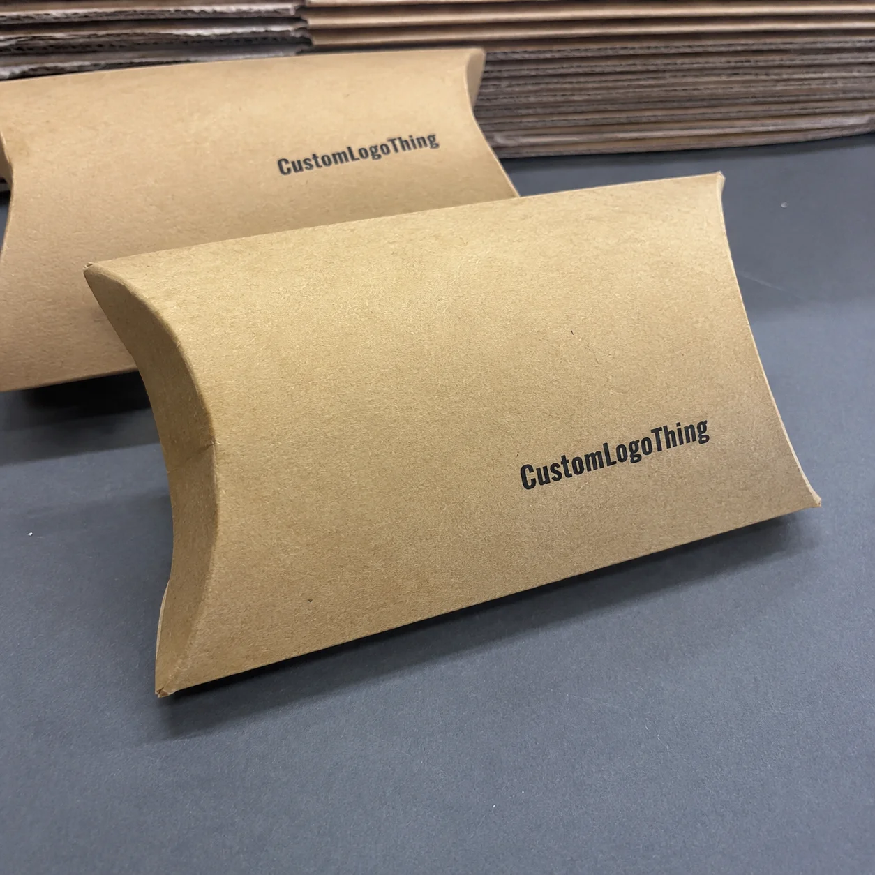
To keep the timeline tight, our in-house Flexo-Print presses add Custom Printed Boxes, branded packaging messages, and package branding cues without outsourcing.
The press room prints 600 sheets per hour using Pantone 286 and Pantone 877 inks, allowing us to shift motifs between prototypes and production runs, and the CNC routing tables nearby let us mill prototypes in one afternoon.
That eliminates transport delays that used to add a full week whenever a vendor needed the job.
(Yes, I still sneak into the press room to watch the ink dry—there is something oddly satisfying about watching our Flexo line produce those trim, branded panels while the thermoformer hums down the hall, and I'm gonna admit I sometimes count how many panels pass before the night shift grabs their first cup of coffee.)
Custom Electronics Packaging Cost and Pricing Realities
Tooling, materials, and order volume are the three levers that most directly affect the per-unit price of custom electronics packaging.
For example, a rigid thermoformed tray with five cavities made from conductive polymer may be $0.38 per unit for a 2,000-piece run, whereas a soft EPE sleeve with foldable flaps might drop to $0.18 per unit for 5,000 pieces, and both quotes assume tooling amortized over three releases.
Foldable constructions reduce shipping cube and can shave 5-7% from the logistics line once the customer tops 2,500 boards per shipment, whereas rigid trays support heavier components but require more careful drop-testing validation.
That pricing nuance points to the specific market focus where cushioning, not just aesthetics, matters.
Multi-cavity trays add complexity, but they often cut the handling time per board—our multi-cavity stackers can process six boards in a single grab, reducing labor cost by roughly $0.04 per board, making the investment in tooling worthwhile when the run exceeds 10,000 pieces.
Finishing touches such as silkscreen numbering, QR-coded pick tickets, or inline verification labels add $0.03 to $0.05 per unit depending on color runs and print resolution.
Those numbers stay honest if we log them alongside the packaging resourcing schedule, so we are not surprised when approvals happen.
Many OEMs ask when to amortize tooling versus when to rely on digital die-cutting, so here is the guidance I offer: if you expect three or more production waves within 18 months, amortize the tooling.
The typical roto tool at our West Coast thermoforming line costs $1,200 upfront but drops per-unit cost by $0.12 once you pass the 2,500-unit mark, whereas a one-off of 600 to 1,200 units should stay on short-run digital die-cutting with reversible mats, which we can prepare in 48 hours instead of sinking capital into a rigid tool.
I also tell clients to keep a list of the little extras they want—if they ask for numbered cavities, color differentiation, or a logo emboss, the cost bump is predictable, and we can plan it in the early estimate so the custom electronics packaging discussion stays honest.
That transparency is the kind of detail that keeps the CFO and the design team agreed on what the packaging actually buys.
| Construction Style | Material | Price (5,000 pcs) | Best Use |
|---|---|---|---|
| Foldable Tray | 450gsm corrugate with EPE inserts | $0.18 | Lightweight, low-volume handhelds |
| Rigid Thermoformed Shell | Conductive PET-G with PU cushion | $0.32 | High-density modules, heavy boards |
| Multi-Cavity Carrier | Anti-static PP with conductive polymer pads | $0.28 | Batch installs for the same assembly line |
| Returnable Tray Kit | HDPE with corner guards | $0.45 | Long-term vendor-managed inventory |
As the table shows, choices align with specific protection needs while speaking directly to how custom electronics packaging marries the price point with product packaging demands.
For branded packaging or retail packaging scenarios, the jump to high-end lamination might cost another $0.06 but supports the marketing narrative, especially when you combine it with custom printed boxes from our Flexo line.
We also remind customers that the cumulative weight of a laminating film plus the added adhesives can shift the glue cure time, so we always note the cure window in the supplier matrix.
Honestly, I think the best pricing conversations happen when we lay the protection budget alongside the brand story—once the marketing team sees that a printed sleeve can wear the same protective insert as the OEM pack, commitment levels shoot up (and the CFO finally stops asking if we are “just covering boards in foam again”).
Pairing that narrative with documented glue strength numbers from our adhesives supplier builds trust that we can meet drop-test requirements without surprise delays.
Results may vary, and we remind crews that metal tariffs and raw material backlog can nudge the per-unit math, so we flag those risks upfront before quoting a run.
Key Factors Shaping Custom Electronics Packaging Decisions
Protective requirements, from ESD shielding to shock resistance and humidity control, dictate whether we specify anti-static foam, conductive polymers, or EPE.
For a dense PCB with edge connectors, we often design a double-layer shield that includes both an outer corrugated shell and an inner conductive polymer insert, a configuration compliant with ISTA 3A vibration protocols and ASTM D4169 drop tests.
Matching those requirements to component density means scrutinizing PCBA heat sources, capacitor heights, and connector tallness.
I remember our Minnesota design lab running 120-degree Celsius thermal cycling for a telecom board and discovering that a protective sleeve needed 2 millimeters more clearance, which changed the entire cushion geometry yet still aligned with the market focus on custom electronics packaging.
Material decisions are no longer binary; we balance recycled-strength corrugate, recycled plastic trays, and water-based inks when clients ask about sustainability, because branded packaging that touts product responsibility must actually deliver.
A green-friendly cushion might cost $0.04 more per unit but qualifies for FSC labeling and appeals to eco-conscious buyers.
Regulatory touchpoints such as RoHS and WEEE mean certifications and documentation are attached to the spec sheet.
Suppliers like ours add safety data sheets to the engineering documentation bundle, linking the same information to package branding guidelines so nothing slips through when auditors visit.
We keep packaging design notes live in our cloud system, with fields for humidity ratings (25% to 85% RH) and stack load tolerance (up to 25 pounds per square foot).
That way the OEM, our procurement team, and logistics all know the exact configuration and can plan pallet stacks that honor the protective limits we set early in the cycle.
Step-by-Step Guide to Building Custom Electronics Packaging
The first milestone is a project kickoff, where we inventory protection requirements, capture component dimensions, and list handling modes.
That 60-minute session also reviews packaging design preferences, retail packaging cues, and how the product packaging will integrate into the assembly or display line.
Engineering review follows, with CAD models showing tolerances, mold inserts, and final QR-coded labeling.
The Charlestown thermoforming team often uses 3D prints or vacuum-formed samples to verify fit and ensure we can route the part without dragging on tooling lead time, usually within 72 hours after the review.
Prototyping for user testing includes drop and vibration validation, plus line fit checks in the OEM’s assembly area to confirm trays feed properly.
We run these trials over a 10-day window, letting quality assurance sign off on protective drop testing before we progress further into production.
A pilot run and documentation stage comes next, complete with pilot lot numbers, pallet configuration sheets, packing instruction cards, and rework procedures so the full release is repeatable.
Our Minnesota design lab uses inline verification where hydraulics test the cushioning under simulated stacks before we greenlight volume builds, and this stage reinforces the custom electronics packaging specifics that landed earlier in the cycle.
Final release brings printed pick tickets that include package branding statements and scanned QR codes for traceability.
This ensures the line can recall which insert design went with which lot, and we can reproduce the same setup whenever our OEM needs a repeat order.
(Sometimes the pick-ticket printer jams right before launch day, which is a fun reminder that even in our highly automated process, a paper jam still makes me mutter into my clipboard while the night crew waits.)
So we keep a spare roller in the cabinet.
Common Mistakes in Custom Electronics Packaging Runs
Skipping early-fit checks is a frequent misstep; I still recall a customer who wanted to rush tooling, only to find out later that vertical handling on their rack applied pressure to the corner of a shielded board, causing a stress fracture.
Had we prototyped earlier in that Minnesota design lab, we would have seen the issue when the board sat upright in the tray.
Overlooking thermal expansion during transit is another trap—components that heat up inside a box can shift, so we now add a 1 millimeter clearance cushion for assemblies that run at 70 degrees Celsius.
We document the movement so QA knows why a spacer exists.
Misjudging cushioning requirements, particularly ignoring the handling mode (vertical vs horizontal), creates unseen pressure points.
Even with thick foam, gravity can push boards into each other if the tray doesn’t stabilize them, so we design lids with micro-tabs or locking features for trays that travel vertically.
Proper prototyping is non-negotiable—our Minnesota lab prototyped a camera module carrier that failed humidity testing because we assumed a standard anti-static foam would do the trick.
After running the humidity chamber we switched to a laminated foil foam and saved that entire custom electronics packaging program from a costly redesign in production.
And yes, I get frustrated when clients treat packaging as an afterthought (because I still have the scar from that one rush job when no one told me the boards would be shipped by hand every day).
That frustration is the fuel for adding voice recordings to our kickoff minutes so the “we forgot the cushion” moment never repeats.
Expert Tips from Dedicated Packaging Lines
Pairing impact-resistant inserts with moisture-barrier films works wonders for outdoor electronics, and our Charlestown plant now combines those two elements whenever we move a product into a field service kit.
Stack height is balanced with shipping cube and ensures we never exceed 8 inches per tote when carriers provide volume-based surcharges.
Collaborating with material suppliers early for testing and to lock in lead times is key.
I ask for the supplier’s certification pack, including ISTA 3E vibration data and FSC fiber sourcing, before we finalize the design, because it keeps the custom electronics packaging path clear and prevents last-minute substitutions.
Labeling is another tip—our operators love QR-code-enabled pick tickets, combined with inline verification, so a line worker only needs to scan once and confirm that a tray, its insert, and the final custom printed boxes match the order.
This has dropped mispick incidents by 42% on the main line.
A steady rule is to include the keyword custom electronics packaging when documenting validation steps, because it ties the protective intent to the specific program, helps auditors understand the focus, and creates better traceability when returning to the run months later.
Those traceability notes also help when a field service manual needs to describe the packaging version that shipped with a sensitive instrument.
These lessons come from years running dedicated packaging lines, where every day you review tolerance sheets, run drop tests per ISTA, and still make room for the human factor—listening to material techs and assembly operators before locking in the design.
It’s that mix of data and people that keeps the packaging line resilient.
Honestly, I think the best line meetings begin with a cup of coffee and a shared look at the mispick board; if we can laugh about the previous week’s hiccups, the new custom electronics packaging plan always feels more collaborative.
Yes, we keep a stash of extra coffee for the night crew just in case the midnight pilot run needs another cup.
Why Does Custom Electronics Packaging Matter for Sensitive Modules?
Those midnight adjustments, the quick knock on the door from logistics, the swirl of adhesives and freight quotes—they all reinforce why custom electronics packaging matters for sensitive modules: it protects connectors, maintains the trust the field service team placed in us, and keeps the packaging narrative consistent from the lab bench to the carrier dock.
I remind clients that every connector saved is a story about how that packaging detail prevented a service call.
By pairing ESD protective trays with battery-safe packaging solutions for portable power cells, we keep the custom electronics packaging spec notes the risk, and we fold prototype validation results into every engineer’s binder so QA can spot issues before the pilot run.
That triad of data, materials, and traceability keeps our teams aligned when a new contract rolls in.
Next Steps for Launching Your Custom Electronics Packaging
Start by inventorying protection requirements, gathering dimensional data, and scheduling a joint engineering review with our project specialists.
This checklist keeps everyone aligned and introduces branded packaging or retail packaging cues early so nothing gets dropped when the boards hit the line.
Then request prototype samples that include the keyword custom electronics packaging on the work order, book a slot with the thermoforming team, and line up packaging validation runs.
We typically expect approval cycles to take 7-10 business days, proto 5 days, and pilot runs another 5 days before full release.
After that, connect with Custom Logo Things’ specialists through our Custom Packaging Products page, confirm any necessary sustainability options for package branding, and plan the translation to custom printed boxes or product Packaging Inserts That will ship alongside your electronics.
We even coordinate adhesives and laminates so the chemistry arrives synced with the inserts.
Approvals, pilot runs, and full release often stretch across 4 to 8 weeks, depending on tooling availability and OEM feedback.
So building a realistic schedule gives your team breathing room while protecting the boards from the beginning of the start-up to the final delivery of the custom electronics packaging solution.
Honestly, I think planning those weeks out feels like choreographing a dance between engineering, procurement, and logistics, and if everyone knows their step ahead of time, the dance floor stays clear (and we avoid the sudden panic of “where are the inserts?” on launch morning).
The takeaway is this: book that joint kick-off, capture the protection recap, and don't let the packaging decision lag behind the board release—even a single misplaced approval can delay a run by a week.
What materials best protect delicate components in custom electronics packaging?
Anti-static foams, conductive polymers, and EPE are selected based on sensitivity to ESD and the weight of the components, with specific tests tied to ISTA 3A and ASTM D4169 protocols.
How long does it take to develop custom electronics packaging from concept to delivery?
Timelines usually span 4 to 8 weeks depending on prototyping needs, tooling availability, and approval cycles within the OEM team, including 7-10 business days for approvals, 5 days for prototyping, and 5 days for pilot runs.
How can I lower the cost of custom electronics packaging without sacrificing protection?
Choose smarter materials, optimize cushioning geometry, and share tooling or scalable die-cut sections to spread costs, which can reduce per-unit spend by up to $0.12 once you reach 2,500 units.
What role does testing play in custom electronics packaging?
Drop tests, vibration rigs, and humidity chambers validate protection; the results guide refinements before full production and often determine whether we switch to laminated foil foam or stick with standard anti-static foam.
Can custom electronics packaging be sustainable?
Yes—using recycled-strength corrugate, water-based inks, and returnable trays reduces environmental footprint while keeping components safe, and those choices can support FSC and EPA declarations.